Overclock.net banner

My first AMD delid and already have doubts/questions

2.6K views 42 replies 14 participants last post by  Donquidik  
#1 · (Edited)
Hello,

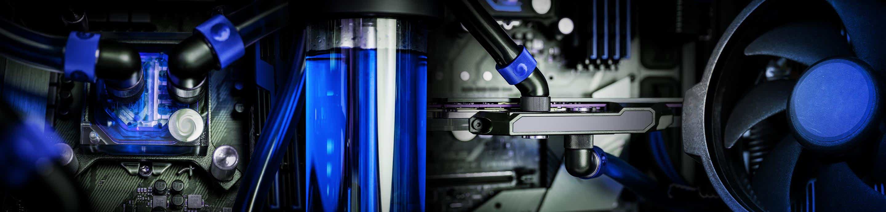
today i received some fun stuff:
  • Delid Die Mate
  • AMD Mycro Direct Die Pro
  • Conductonaut extreme
  • some tubing and new fittings

I delidded already a couple CPU
(3770K/6700K/7700K/13900KF/14900KF/14900KS and some more for my friends)
So i think at least i know what i´m doing...

But i was still careful and before i sacrify my 9950X3D i´ll
gave it a shot on my 7600X3D.
and probably this was the best decission i made in the last months:

this is what the I/O die now looks like:


here is the total of the delidded CPU:


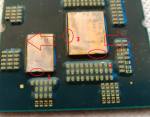
you can clearly see damage in the marked spots:


Spot 3 could be from the delid process but for 1 and 2
I have no explanation.
The delidder moves that way:


Did anyone of you discover the same or a similar issue with deliding?
 
#2 ·
I not delided anything that modern but I seen dies with far more damaged that still worked fine. Back when lapping was all the craze some folks even lapped dies with sandpaper. you can remove a lot more off the die then you think before you run into problems, that being said it might be a good idea to fill or sand down the chips, last thing you want is a stress crack forming from all the heat cycles.
 
#3 ·
I've delidded a couple of Granite Ridge CPUs with the TG Delid-Die-Mate, with no damage.

I'm not sure what could have resulted in cracking/spalling like that. The solder shouldn't be hard enough, nor so securely attached that it's ripping pieces off the dies. Almost makes me think there was pressure from underneath during the process, or that the whole CPU was bent or hit in such away that caused damage before the delid was even attempted.

You didn't chill the part or something, did you?


Problem with damage this deep is that it can't be lapped off. The SMDs around the dies are almost the height of the die already and it doesn't take the removal of much material to either hit them while lapping, or to prevent a cooler from sitting flush.
 
#4 · (Edited)
I seen dies with far more damaged that still worked fine
I´m also prety confident it will still work, i just never seen damage like that after a delid.
Maybe it was before, i just used the delidding tool and cleaned one step with liquid metal.

You didn't chill the part or something, did you?
Chilled? brought the temp down? no, more in the upper room temps today 😅

What i also can say, i needed close to no force for the first movement of the IHS. Was pretty easy.

@der8auer
sorry for tagging you, but maybe your the best to ask. Did you ever seen that kind of damage from a delid?
 
#5 ·
The old razor blade and lighter is still by far the best delidding method out there still. These delid kits that just try to fatigue the solder off the dies is just asking for trouble. Trouble like this.

cut the glue. Heat the IHS till solder melts and IHS falls off. Done and no risk to dies.
 
  • Rep+
Reactions: PLATOON TEKK
#7 · (Edited)
You may get lucky. They do the circuit stuff on the bottom of the silicon not the top. If it was the other way it would be instant death. I don't know if the way they do x3d is to put traces on both sides of the silicon or not. If yes you are very possibly boned, but I don't know how it is done. If it goes do one set of traces, deposit something, do the other set, they're BOTH on the bottom-and as long as no traces are touched or crushed, it may work just fine. People do delid x3d chips though which strikes me as just too dangerous if they’re top/bottom though.
 
#8 · (Edited)
You may get lucky.
I will see today if it is still running... would be a shame if not... could go CO -45 on it, bench and game stable, just when it were idle to long it rebooted :ROFLMAO:
Here is a update to position 2 in the Pictures in the first post:

But I´m still a bit worried, did it come from delid orwas it before maybe.

Delid process was so easy, just needed 2 fingers to turn the allen key.
Totally smooth, no crackling noise, nothing. Just like a walk in the park.
 
#9 ·
you sand at a angle. he only needs to chamfer the edges to keep it from cracking over time
This is an actual picture of the under side of a Raphael CCD:
Image

Entire thing is 10.7mm* 6.75mm and it needs to dissipate 120W+ at peak loads, almost all of that from the outer portions of the cores, away from the caches, where the hottest execution units are.

There is virtually no margin from the edge of the die before you are directly over active transistors; 0.08mm die spacing is typical at this scale. Chamfer the edges and you move some of the hottest parts (the FPUs are on the narrow sides of the CCD) of one of the most power dense modern ICs, away from the underside of the IHS, probably negating all of the advantages of the de-lid in the first place.

Bondline thickness of liquid metal TIM on an intact die and a flat cold plate is normally on the order of 30 microns. Taking a third of a mm off the edges is going to increase that about ten fold.

You may get lucky. They do the circuit stuff on the bottom of the silicon not the top.
They don't. The upper ~90% of the CCD's Z-axis, even on the v-cache parts, is solid structual silicon.

I will see today if it is still running... would be a shame if not... could go CO -45 on it, bench and game stable, just when it were idle to long it rebooted :ROFLMAO:
Here is a update to position 2 in the Pictures in the first post:
View attachment 2714817
But I´m still a bit worried, did it come from delid orwas it before maybe.

Delid process was so easy, just needed 2 fingers to turn the allen key.
Totally smooth, no crackling noise, nothing. Just like a walk in the park.
I suspect it still works, but that it won't stay that way in real use, and I strongly suspect trying to chamfer the edges will ruin load temps.

Where did you originally get this CPU?

Normally there is some initial resistance on the delid. That you encounted none could suggest that the glue was already cut and/or that the solder interface was already damaged.
 
#15 ·
This is an actual picture of the under side of a Raphael CCD:
Image

Entire thing is 10.7mm* 6.75mm and it needs to dissipate 120W+ at peak loads, almost all of that from the outer portions of the cores, away from the caches, where the hottest execution units are.

There is virtually no margin from the edge of the die before you are directly over active transistors; 0.08mm die spacing is typical at this scale. Chamfer the edges and you move some of the hottest parts (the FPUs are on the narrow sides of the CCD) of one of the most power dense modern ICs, away from the underside of the IHS, probably negating all of the advantages of the de-lid in the first place.
I'm not sure what you're on but there is enough meat there is sand a bit off the chips in the die to prevent stress cracking.
 
#10 ·
#12 ·
That you encounted none could suggest that the glue was already cut and/or that the solder interface was already damaged.
Might have been damaged when you bought it. Did you see any signs that this wasn't the first time the lid had been detached, other than the lack of resistance?
No other signs or marks, I also used the CPU stock before...
The slider moved super easy from the beginning but still had to move it 50-60 times forward and back to release the IHS completely.
That what should be typical, at least what i have read about ryzen delid...
 
#13 ·
I´m not that worried about the CCD due to the fact it is a Ryzen 7000 with 3D cache on top and filler to the sides:
Image
 
#14 ·
You may get lucky. They do the circuit stuff on the bottom of the silicon not the top. If it was the other way it would be instant death. I don't know if the way they do x3d is to put traces on both sides of the silicon or not. If yes you are very possibly boned, but I don't know how it is done.
I will see today if it is still running... would be a shame if not... could go CO -45 on it, bench and game stable, just when it were idle to long it rebooted :ROFLMAO:
Here is a update to position 2 in the Pictures in the first post:
View attachment 2714817
But I´m still a bit worried, did it come from delid orwas it before maybe.

Delid process was so easy, just needed 2 fingers to turn the allen key.
Totally smooth, no crackling noise, nothing. Just like a walk in the park.
if you got it to boot in the first place and it didn’t just hork and die when you tried, you’re probably good. processor faults are like that. Theres too many computations per second for it to be subtle. Since I don’t know how the 3d cache works filling it to the brim may not be a bad idea. Memory errors are like that. Thing works great till you hit the buggered bit then all hell breaks loose. If it lives through that then I don’t foresee any future issues.
 
#18 ·
Sad news, she´s dead...
 
#19 ·
Normaly these tool is bullet proof, was new (first delid with this tool) CPU was in working condition before.

So what went wrong?
 
#20 ·
Very weird that you had such an issue. Reallly bad luck and I feel your pain as I have killed a 14900k from lapping the die in a wrong way… Had to pay for that mistake , opened my wallet and payed for a brand new one next day which I delidded and lapped in a correct way this time 😅

With soldered CPUs there is always a risk by doing this with no heat. If you heat the cpu at 170c the solder will melt and the delid will be easy peasy , that’s what we did for the Ultra series !

Before doing this on an AMD cpu make sure that it can withstand such temps with no issues because I am not tuning AMD CPUs so that I don’t know.
 
#21 ·
Actually i´m happy i started with my 7600X3D, thats not that big of a loss, but there can be so many variables, fragile CPU, maybe i did something wrong
(can´t imagine what i can do wrong when turning a screw...) maybe the tool is off or just bad luck...
 
#22 ·
I´m not that worried about the CCD due to the fact it is a Ryzen 7000 with 3D cache on top and filler to the sides:
View attachment 2714819
That image is a demonstration mock-up and not what the CCD actually looks like. You can't see the spacers on the sides because there is another layer of silicon over it.

The side spacers are about ~10 microns thick and are underneath a single ~1000 micron thick piece of silicon that covers the whole thing.

I can’t tell if this is a confirmation or dispute. You say no, then describe it as if it is correct. May not matter. I’m currently going with one of us (not sure who) rolled a one on their reading or writing Skill check.
There is negligible risk of damaging the transistors by carefully chamfering the edges of the CCD. There is a lot of silicon on top of the active dies.

However, chamfering the edges of the CCD will almost certainly result in elevated thermals, because you'd be dramatically increasing the gap the TIM has to fill to conduct heat from the hotter parts of the CCD to the cold plate.

No other signs or marks, I also used the CPU stock before...
The slider moved super easy from the beginning but still had to move it 50-60 times forward and back to release the IHS completely.
That what should be typical, at least what i have read about ryzen delid...
Normaly these tool is bullet proof, was new (first delid with this tool) CPU was in working condition before.

So what went wrong?
I have a suspicion that a previous owner delidded the part, did some minor damage to it, and then reattached the lid by using dabs of liquid metal (which can alloy with the solider left under the IHS and re-solidify once the gallium diffuses into the indium sufficiently to no longer be liquid at room temperature). The you buy this part and unwittingly finish it off it with the stresses of the second delid.

It's also entirely possible that the mechanical and thermal stresses involved in relatively normal use started cracks that ensured it wouldn't survive the delid.

Or perhaps you just got really unlucky. There are probably several dozens, if not hundreds of Raphael/Granite Ridge delids via this method for every one that results in a failed CPU, but it's certainly not impossible to kill one.
 
#27 ·
That image is a demonstration mock-up and not what the CCD actually looks like. You can't see the spacers on the sides because there is another layer of silicon over it.

The side spacers are about ~10 microns thick and are underneath a single ~1000 micron thick piece of silicon that covers the whole thing.


There is negligible risk of damaging the transistors by carefully chamfering the edges of the CCD. There is a lot of silicon on top of the active dies.

However, chamfering the edges of the CCD will almost certainly result in elevated thermals, because you'd be dramatically increasing the gap the TIM has to fill to conduct heat from the hotter parts of the CCD to the cold plate.


I have a suspicion that a previous owner delidded the part, did some minor damage to it, and then reattached the lid by using dabs of liquid metal (which can alloy with the solider left under the IHS and re-solidify once the gallium diffuses into the indium sufficiently to no longer be liquid at room temperature). The you buy this part and unwittingly finish it off it with the stresses of the second delid.

It's also entirely possible that the mechanical and thermal stresses involved in relatively normal use started cracks that ensured it wouldn't survive the delid.

Or perhaps you just got really unlucky. There are probably several dozens, if not hundreds of Raphael/Granite Ridge delids via this method for every one that results in a failed CPU, but it's certainly not impossible to kill one.
So confirmation plus chamfering info. My suspicion is the chamfering is necessary to keep any microcracks from happening. They used to do something like that with hockey rink lexan. Drill a big round hole in the end of the crack. Kept the crack from propogating.
 
#23 ·
have to gain my courage back together till Sunday, there my plan was to actually delid the other one...
At the moment, I consider to send back the micro direct die pro and the delidder 😅
 
#24 ·
Delid process was so easy, just needed 2 fingers to turn the allen key.
Totally smooth, no crackling noise, nothing. Just like a walk in the park.
When I delided my AM5, it was not easy or smooth. Certainly needed more than two fingers to turn the allen key.

I bought it used on ebay, according to receipt, 2 month old.
Did you test it before deliding?

Normaly these tool is bullet proof, was new (first delid with this tool) CPU was in working condition before.

So what went wrong?
Good question... That damage should not be possible with the delid. Looks like someone tried to mount a CPU cooler directly on the die and overtightened or didn't tighten evenly.

Sad news, she´s dead...
Yeah.... Those pictures held no hope :(
 
#25 ·
Is it possible you chipped it while scraping off the indium? I have had issues like that in the past (OLD AMD CPUs) with rough handling of the die. The corners are very fragile, easy to chip while scraping.
 
#26 ·
I used the little "cpu cleaning tool"
to remove the glue:

and the biggest amount of the Indium:


So there is also a little possibility that I f.....ed it up...

all the times before i used a razor blade to clean of the indium down to the die....
 
#34 ·
I delidded mine 9950x3d.
As like you i had serious doubt, my 14700kf did go wrong with the tool from EK it broke the complete die off after about 25 minutes going back and forward.
I decided to brake the glue going back and forward 4 times. Than i took a solder gun and heated up the ihs. It took forever at 170c and it did not come loose.
So i got a temperature probe and i found out the ihs was only getting 120c. Setting the gun to 500c helped.
At exactly 155c the ihs fell of the die.
It felt smooth and save and i am happy i did it this way, everything is working great.
 
#35 ·
Will delidding help require lower vsoc if I drop temps 20c? I guess I could test beforehand but lowering the GHz and voltage manually.
 
#41 ·
~3hrs and 4 pair of underpants later, I successfully delidded my 9950x3d 😰 theres a delta of 10° from coldest to hottest core under full load, so when i redo the loop in a couple weeks i have to reaply LM, but for now i´m happy
 
  • Wow
Reactions: HippoLOL
#42 ·
I had a pair full of bricks too... when I got zero on first boot attempt...
Turned out the water block was not tightened down enough. Once I figured that out I was looking at the idle temp in BIOS and wasn't that impressed (~45C), but come to find out that is normal for this chip. I used liquid metal to dissolve the indium and then some conductonaut extreme. Finally, after everything was done, I was really impressed. I'd estimate it was a drop of 20C from what you normally see. Once I got a chiller on it (only 13-15C since it's humid here these days), I almost never, ever hit 60C. It took about 30 slides with the TG delidder before it got loose. At first I was a little concerned as to whether the chamfering was how it should look, but I asked TG based on some pics, if that was normal. I want to say there was what looked like a tiny nick or two on some edges, but it all worked in the end.